


KD-KA01
Cecelia is an accomplished electrical engineer with expertise in automation and control systems. She is a natural problem-solver and thrives on developing solutions that optimize performance and efficiency.
TPS5430/TPS5431 dc/dc converter integrating high side N-channel MOSFETs with low resistance, which is designed to provide up to 3A output from an input voltage source of 5.5V to 36V (TPS5430) or 5.5V to 23V (TPS5431). The substrate includes a voltage error amplifier with high performance which is used to provide tight voltage regulation accuracy under transient conditions, an undervoltage lockout circuit used to prevent start-up until the input voltage reaches 5.5V, an internally programmed slow-start circuit designed to limit surge current, and a voltage feedforward circuit designed to improve transient response. It also provides a sensitive high enable, overcurrent protection, and thermal shutdown. It has an internal feedback compensation loop to reduce design complexity and external component count.
The TPS5430/TPS5431 devices are packaged in a thermally enhanced, easy-to-use 8-pin SOIC Power Strip™. TI offers evaluation modules and design software tools to help quickly implement high-performance power designs to meet intense device development cycles. The TPS5430/TPS5431 has a switch enable pin with only 17μA quiescent current in the off state. Compared with other DC switching power conversion chips of the same type, the high conversion efficiency of TPS5430/TPS5431 is particularly noteworthy.
TPS5430/TPS5431 can be used to power the A/D conversion module and data processing module of the data acquisition system.
TPS5430 has good characteristics, and its performance and main parameters are as follows:
High current output: 3A (peak 4A);
Wide voltage input range: 5.5~36V;
High conversion efficiency: the best condition can reach 95%;
Wide voltage output range: the lowest can be adjusted down to 1.221V;
Internal compensation minimizes external component count;
Fixed 500kHz conversion rate;
With over-current protection and thermal shutdown function;
With switch enable pin, only 17uA quiescent current in an off state;
Compared with other DC switching power conversion chips of the same type, the high conversion efficiency of TPS5430 is particularly noteworthy.
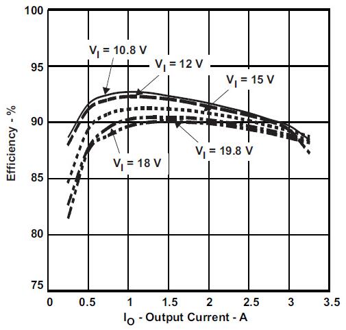
The figure below shows the relationship between TPS5430 conversion efficiency and output current at 12V input voltage and 5V output voltage.
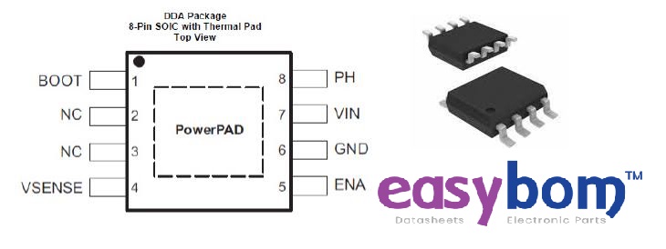
a. Pin description
TPS5430 adopts 8-pin SO IC PowerPADTM package, and the form is as shown below.

b. Internal structure and function
① Oscillator frequency
A fixed slew rate of 500kHz results in a smaller output inductance for the same output ripple requirement.
② Reference voltage
Scale the temperature to stabilize the output range of a bandgap circuit, making the quasi-voltage system produce an accurate reference signal. After testing, within the allowable temperature range, the bandgap and scaling circuit remain balanced when the 1.221V voltage is output.
③ ENA (enable pin) and (SlowStart) internal soft-start
When the voltage on the pin ENA exceeds the limit voltage, the converter and the internal soft-start begin working, and when the voltage is lower than the limit voltage, the converter stops working and the soft-start begins resetting. The converter stops working when the pin ENA is grounded or the voltage is less than 015V. The ENA pin can be left floating.
④ UVLO (Under Voltage Lockout)
TPS5430 has a UVLO circuit. No matter in the power-up or power-down process as long as V IN (input voltage) is lower than the limit voltage, the conversion chip does not work. The typical hysteresis value of the UVLO comparator is 330mV.
⑤ Boost Capacitor (start capacitor)
Connect a 0.01μF ceramic capacitor between the BOOT pin and the PH pin to provide the gate voltage for the high side of the MOSFET.
⑥ VSENSE (external feedback) and Internal Compensation (internal compensation)
The output voltage is fed back to the VSENSE pin through an external resistor divider. In a steady-state, the voltage of the VSENSE pin is equal to the voltage reference value of 1.221V. The TPS5430 has an internal compensation circuit, which simplifies the chip design.
⑦ Voltage Feed Forward
The internal voltage positive feedback ensures that the power chip has a constant gain no matter how the input voltage changes. This greatly simplifies stability analysis and improves transient response. The positive feedback gain of the TPS5430 is typically 25.
⑧ Pulse - Width - Modulation Control
The converter adopts a fixed frequency control method.
⑨ Overcurrent Protection
The overcurrent protection circuit makes the internal overcurrent indicator set to true when the current exceeds the limit value, and the overcurrent protection is triggered.
⑩ Thermal Shutdown
The junction temperature exceeds the temperature shutdown point, the voltage parameter is set to ground, and the high-side MOSFET turns off. Controlled by the soft-start circuit, when the contact temperature drops to 14°C lower than the temperature shutdown point, the chip restarts.
In the power supply design process, the design parameters should be determined first according to the work requirements, and then the circuit and peripheral components should be designed according to the parameters.
(1) Design parameter requirements
Input voltage range: 10.8~19.8V;
Output voltage: 5V;
Input ripple voltage: 300mV;
Output ripple voltage: 30mV;
Output rated current: 3A.
(2) Application circuit
The power supply design of this system selects the classic circuit of TPS5430, as shown in the figure below.
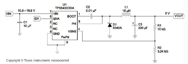
5V output voltage application circuit diagram

5V output voltage application circuit diagram under wide voltage input
(3) Selection of components
①Input capacitor
The TPS5430 requires a slightly larger decoupling capacitor. A high-performance ceramic capacitor of 10µF (C1) is recommended here. Smaller capacitors can also be selected, subject to the input voltage and rated current ripple requirements.
② output filter device
The output filter device, namely L1, C2. TPS5430 has an internal compensation circuit. The output inductance is related to the maximum output current, and a 15μH inductor is selected here.
Output capacitance is an important design factor that affects voltage rating, ripple current rating, and equivalent resistance (ESR). In this application, a 220μF output capacitor is selected. At this time, the RMS ripple current generated in the circuit is 143mA, and the maximum ESR required is 40MΩ.
③ Output voltage setting
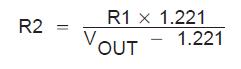
The output voltage is determined by the resistors (R1, R2) of the VSENSE pin. If the output voltage is 5.0V, the reference voltage is 1.221V, and R1 is 10kΩ, then R2 is determined to be 3.24kΩ.
④ BOOT capacitor
BOOT capacitor C2 select 0.01μF.
⑤ Capture diode
TPS5430 needs an external capture diode, choose B340A, its reverse voltage is 40V, forward current is 3A, and forward voltage is 0.5V.
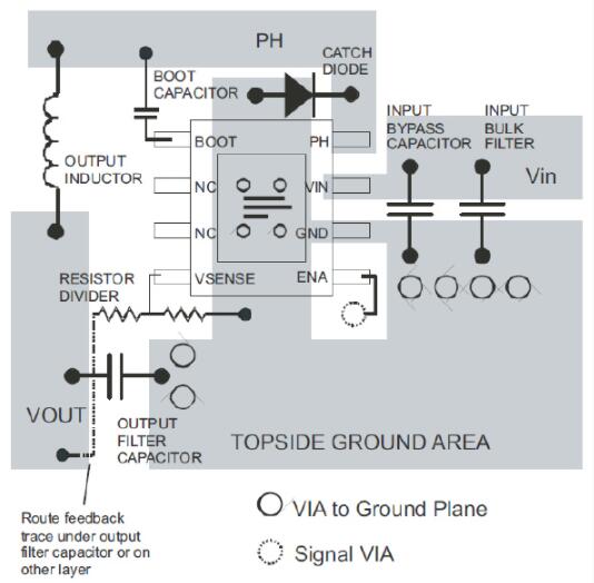
TI recommends the circuit board wiring and component placement diagram of the 10.8~19.8V input to 5V output voltage of the TPS5430, as shown in the figure.
In the circuit board design process of TPS5430, the design principles of general power conversion chip circuits should be followed to achieve the expected results. There are two other things to note:
① PowerPAD is required to be connected to the ground. The Pads can be placed directly under the chip, and vias can be drilled to facilitate heat dissipation.
②If there is no special requirement for the ENA pin, it can be left floating, or a signal via hole can be reserved.

Cecelia is an accomplished electrical engineer with expertise in automation and control systems. She is a natural problem-solver and thrives on developing solutions that optimize performance and efficiency.

 Anita · March 22,2022
The MAX232 IC is a type of dual receiver. It is used for TTL/CMOS to RS232 conversion. Most microcontrollers operate on TTL/CMOS logic. Therefore, it communicates through either 0V or +5V.
Electronic Component Parts ArticlesAccess:7537

Cecelia · February 28,2022
LM741 is a general-purpose operational amplifier with a very wide range of applications. It can be used in various digital instruments and industrial automatic control equipment.
Electronic Component Parts ArticlesAccess:7884

Anita · February 26,2022
The TPA3118D2 is a stereo-efficient, digital amplifier. The high efficiency of the unit allows it to run 2 x 15W without an external heat sink on one layer of PCB. It can run without a heat sink on a 2 × 30 W / 8 Ω dual-layer PCB.
Electronic Component Parts ArticlesAccess:2338

Anita · February 23,2022
The CD4042BE is a kind of d latch. The types include four latch circuits that are being triggered by a common timer. The outputs of the buffered version are also available in each circuit.
Electronic Component Parts ArticlesAccess:2983
Popular Posts
Hot Labels
Popular Parts