


KD-KA01
Cecelia is an accomplished electrical engineer with expertise in automation and control systems. She is a natural problem-solver and thrives on developing solutions that optimize performance and efficiency.
To obtain the +1.8v output voltage, please use Figure a. To obtain 3.3V, +5V output voltage, please use Figure b.


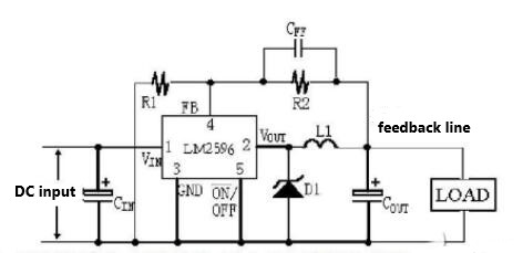
LM2596 supports adjustable output. When the input is 40V, the output can be continuously adjusted to 0~37V. The typical application circuit is as follows:
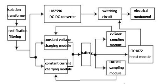
1.1 The overall block diagram of the system
According to the system design requirements, the uninterruptible DC power supply has: when there is no AC power supply, the equipment is continuously powered; when the AC power supply is normal, there are two modes of constant voltage charging and constant current charging. Considering the design requirements, a system block diagram is formed as shown in figure 1.
1.2 The choice of DC-DC converter scheme
Using the switching voltage regulator LM2596, it can output a drive current of 3 A, and has good linearity and load regulation characteristics. It can output three voltages of 3.3 V, 5 V, and 12 V, and it can also realize the adjustable output between 1.2 and 37 V.
The device integrates frequency compensation and a fixed frequency generator with a switching frequency of 150 kHz. Compared with low-frequency switching regulators, smaller filter components can be used. Since the device only needs 4 external components, a general standard inductor can be used, which simplifies the use of LM2596 and greatly simplifies the design of the switching power supply circuit. Under the conditions of specific input voltage and output load, the error of the output voltage can be guaranteed to be within ±4%, and the error of the oscillation frequency is within ±15%. It can use only 80 μA standby current to realize external power-off; it has a self-protection circuit (a two-stage frequency-reduction current-limiting protection and an over-temperature complete protection circuit that powers off under abnormal conditions).
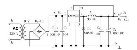
The DC-DC converter circuit is shown in Figure 2.
1.3 Constant voltage charging circuit design
The constant voltage charging circuit is shown in Figure 3. The circuit consists of an operational amplifier LM324 and a three-terminal regulator W117. LM324 is connected as a voltage follower, its output voltage U1 = U- = U+ = UX, it can be seen that the output voltage can be changed by adjusting the middle tap of the resistor R2. Due to the existence of the operational amplifier, the output voltage is adjusted very smoothly.

1.4 Voltage-controlled constant-current charging circuit design
The circuit principle is shown in Figure 4. The constant current source circuit is composed of operational amplifier LM324, field-effect tube IRF640, sampling resistor R3, load resistor RL, and so on.

The circuit uses a high-power field-effect tube IRF640 as a regulator tube, which is an N-channel enhancement type MOS tube. The working voltage of the tube can reach up to 100 V, the saturated drain current can reach 28 A, and the power consumption is about 150 W. When the effect tube works in the saturation region, the drain current Id is approximately the current controlled by the voltage Ugs. That is, when Ud is a constant, it satisfies Id = f (Ugs), as long as Ugs does not change, Id does not change.
In this circuit, R2 is the sampling resistance of the constant wire material (the resistance changes little with temperature). As a voltage follower, OP07 has U+ = U-= Us. Since the gate current is negligible, Id = Is = I2 = Us R2 = U+ R2. Because Id = U+ R2, the circuit input voltage U+ control current Id, That is, Id does not change with the change of RL, to realize voltage control and constant current. The parameter charging current in Figure 4 is 200 mA. If you want to change the charging current, you only need to adjust R2.
LM2596 performance characteristics:
Built-in fixed frequency oscillator (150KHZ) and reference regulator (1.23v)
With complete protection circuit, current limit, thermal shutdown circuit, etc.
Only a few peripheral components are needed to form a high-efficiency voltage stabilizing circuit.
Provide multiple voltage grades such as 3.3V, 5V, 12V, and adjustable (-ADJ).
The conventional application of M2596 does not have the current limiting function. In some electronic designs and auxiliary equipment, there is a certain demand for the current limiting function. Although the standard application circuit given by the manufacturer cannot complete this function, we can add the function circuit appropriately, making it realize the current limiting function. As shown below:

The figure below shows the LED switch constant current stabilized power supply based on LM2596-ADJ.

This circuit contains two loops: voltage control loop and current control loop. The voltage control loop is composed of operational amplifiers U2A, R1, and R5 to control the maximum output voltage of the power supply.

Cecelia is an accomplished electrical engineer with expertise in automation and control systems. She is a natural problem-solver and thrives on developing solutions that optimize performance and efficiency.

 Anita · March 22,2022
The MAX232 IC is a type of dual receiver. It is used for TTL/CMOS to RS232 conversion. Most microcontrollers operate on TTL/CMOS logic. Therefore, it communicates through either 0V or +5V.
Electronic Component Parts ArticlesAccess:7724

Cecelia · February 28,2022
LM741 is a general-purpose operational amplifier with a very wide range of applications. It can be used in various digital instruments and industrial automatic control equipment.
Electronic Component Parts ArticlesAccess:8052

Anita · February 26,2022
The TPA3118D2 is a stereo-efficient, digital amplifier. The high efficiency of the unit allows it to run 2 x 15W without an external heat sink on one layer of PCB. It can run without a heat sink on a 2 × 30 W / 8 Ω dual-layer PCB.
Electronic Component Parts ArticlesAccess:2424

Anita · February 23,2022
The CD4042BE is a kind of d latch. The types include four latch circuits that are being triggered by a common timer. The outputs of the buffered version are also available in each circuit.
Electronic Component Parts ArticlesAccess:3048
Popular Posts
Hot Labels
Popular Parts